
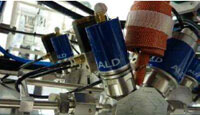
The UW has chosen the AltaCVD™ chemical vapor deposition (CVD) system to develop semiconductor-based devices including CMOS transistors, MEMS, ICs, advanced LEDs and solar cells. The system will be installed at the Washington Nanofabrication Facility (WNF) on the UW Seattle campus, where it will be used by both internal and external researchers. Together with the recently installed advanced deep reactive ion etcher (DRIE) and plasma-enhanced CVD (PECVD) tools, the AltaCVD system provides the capability to assemble an electroplated TSV fill process.
About Altatech
The AltaCVD system was developed by Altatech, a subsidiary of Soitec, a world leader in generating and manufacturing semiconductor materials.
About the Washington Nanofabrication Facility (WNF)
A national user facility that provides full-service, micro- and nanotechnology, the WNF is the largest public-access fabrication center in the Pacific Northwest, with 15,000 square feet of laboratories, cleanrooms, and user spaces focused on enabling basic and applied research, advanced research and development, and prototype production.
See also
- Washington Nanofabrication Facility (WNF)
- Soitec (parent company of Altatech)
- Wall Street Journal MarketWatch