

By Chelsea Yates
Photos by University of Washington
Step inside the Washington Nanofabrication Facility, where tiny tech is transforming research in quantum, chips, medicine and more.
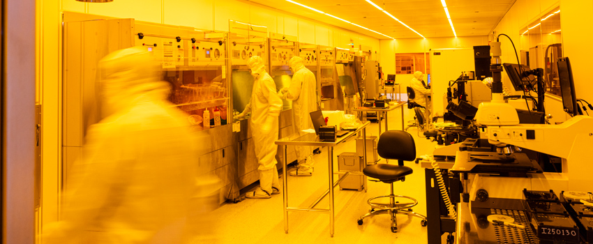
Researchers wear full-body clean suits in the WNF to prevent contamination. The air in this environment is 1,000 times cleaner than in an operating room.
Imagine a high-tech workshop where scientists and engineers craft objects so small they can’t be seen with the naked eye — or even a standard microscope. These tiny structures — nanostructures — are thousands of times smaller than a strand of hair. And they are essential for faster computers, better smartphones and life-saving medical devices.
Related story

WNF student lands his dream internship
Prithvi Krishnaswamy, a senior majoring in electrical and computer engineering, shares how his experiences working at the WNF helped set him up for interning at Nvidia.
Nanostructures are at the core of the research happening every day in the Washington Nanofabrication Facility (WNF). Part of the Institute for Nano-Engineered Systems at the UW and located in Fluke Hall, the WNF supports cutting-edge academic and industry research, prototyping and hands-on student training. Like many leading nanofabrication centers, it is part of the National Science Foundation’s National Nanotechnology Coordinated Infrastructure, a network that shares expertise and resources.
Inside the WNF, which is the largest publicly accessible full-service cleanroom in the Pacific Northwest, researchers work in an ultra-clean environment. They wear full-body clean suits to prevent contamination. This protection isn’t necessarily for the workers but for the environment — the items being made are so small that a speck of dust, strand of hair or drop of sweat could ruin them. The air is 1,000 times cleaner than an operating room, and parts of the facility are bathed in yellow light to protect ultraviolet and blue light-sensitive materials.
Unlike many university nanofabrication labs, which were started by small academic research teams, the precursor to the WNF was founded by the Washington Technology Center as an incubator for companies working in nanotechnology R&D and prototyping. This early investment secured advanced tools from the start. In 2011, the UW took full ownership, and after a six-year, $37 million investment, transformed the WNF into a fully operational cleanroom with over 100 specialized processing and characterization tools.
Today it is critical for advancing semiconductor and quantum research.
A hub for semiconductor innovation
Semiconductor chips power everything from cars to smartphones. The WNF provides the expertise needed to design, build and test these chips, which contain millions of microscopic transistors controlling electricity flow. These components are so small they must be inspected at the nanoscale. Researchers use advanced techniques like photolithography and etching to carve precise patterns on silicon wafers, layering materials to form semiconductors.
Primarily a Micro-Electro-Mechanical Systems (MEMS) fabrication facility, the WNF enables the creation of microscopic devices that integrate mechanical and electrical components to sense, control and actuate on a micro scale — generating macro-scale effects. MEMS devices, including microsensors, microactuators and microelectronics, are fabricated using techniques similar to those used for integrated circuits. Car airbags rely on MEMS accelerometers, while smartphones use MEMS microphones and filters. In addition to MEMS, the WNF has recently begun fabricating chips and integrated circuits for photonics and trains students in critical semiconductor manufacturing skills — essential for expanding U.S. chip production.
“Remember the pandemic-era chip shortage that made buying a car or smart appliance difficult? If we manufacture more chips domestically, then we’ll be less reliant on importing them from other countries,” says WNF Director Maria Huffman. “Chips are critical not just for consumer goods but also for telecommunications — data transmission and processing, 5G networks and IoT connectivity — as well as national security, military systems and supply chain resilience.”
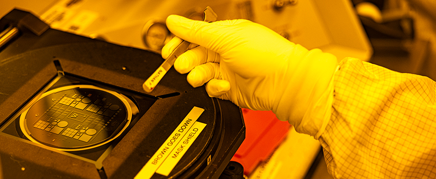
Yellow lighting in parts of the facility protects light-sensitive materials, such as those used on the silicon wafer shown here.
Enabling quantum research
Quantum technologies rely on nanoscale precision to explore and harness quantum phenomena. Quantum computers, for example, use qubits — basic units of quantum information — often built using superconducting materials. The WNF enables researchers to create some of these components with extreme accuracy, depositing ultra-thin layers of materials and fabricating structures at the atomic level.
Quantum systems depend on materials with special properties, such as superconductors — materials with zero electrical resistance — or 2D materials like graphene. Nanofabrication facilities allow researchers to customize the size, shape and composition of these materials. Quantum sensors also rely on nanofabrication for their development. They are used in applications such as ultra-precise timekeeping—including quantum clocks—and advanced navigation systems.
Collaboration on the nanoscale
Nanofabrication facilities like the WNF enable groundbreaking research, from next-generation semiconductors to quantum technology. But maintaining such a facility isn’t cheap — the WNF relies on grants, industry partnerships and user fees to stay at the cutting edge.
“Advancing tomorrow’s technologies isn’t possible with decades-old equipment,” says Huffman. “We need to be cutting edge to drive cutting-edge innovation.” Industry partners like Micron and Intel have contributed funding, Meta has donated equipment, and many others pay to use the facility for R&D and prototyping.
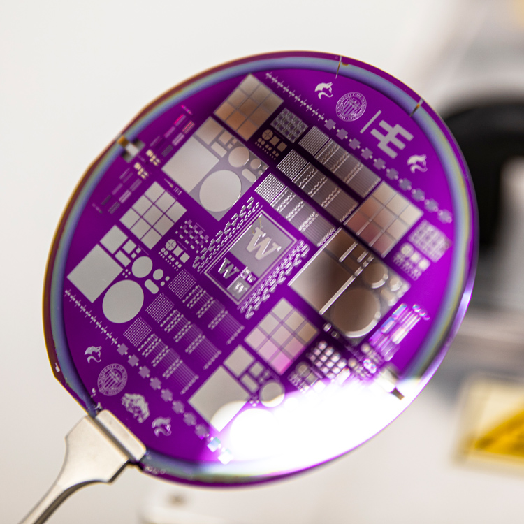
Advanced techniques like photolithography and etching create intricate patterns on silicon wafers like this one. A single 4- or 6-inch wafer can hold dozens of chips, depending on their size.
“Generally, companies aren’t resourced to build their own experimental spaces or disrupt or stop their production lines to try something new,” explains Darick Baker, the facility’s engineering and business development manager. “This is where the WNF can help.”
Beyond industry use, the WNF is deeply invested in education. With support from Micron and Intel, it was one of the first in the Pacific Northwest to pilot introductory semiconductor short courses, which have since been replicated at other universities. This spring, the WNF is hosting hands-on classes where undergraduates — from UW engineering students to veterans in a Bellevue College technical training program — will build basic functional devices on silicon wafers.
“Industry needs people in many roles to be trained to work with nanomaterials — not just engineers and scientists but technicians, maintenance workers and more,” Baker says.
Whether advancing semiconductor research, unlocking quantum potential or training future innovators, collaboration is key. At the WNF, researchers, students and industry partners work side by side, tackling nanoscale challenges to shape the future in big ways.
Want to become a WNF user?
Discover more about the services, equipment and learning opportunities available to students, faculty and industry professionals.
Originally published April 7, 2025